A Preliminary Talk on the Power Supply Circuit Design in Active-Clamp and LLC II : A comparison of pulse input and DC input DC to DC converters
The switching power supplies of personal computers usually have a multiple output voltage design, in which the main output has the maximum current of 12V and is the focus of the power supply design. Secondly, 3.3V and 5V have smaller output currents. In general, DC to DC converters are used to enhance the stability of the power supply output voltage, decreasing from 12V to 3.3V and 5V power supply for computer use. DC to DC is generally divided into two types according to input source: 1. Pulse input DC to DC converters, which can modulate the DC pulse input cycle width to achieve the purpose of DC conversion. However, the control method is relatively complex, and an application limitation is that it is mostly used in a forward topology circuit design; 2. DC input DC to DC converters, which can achieve the purpose of DC conversion by adjusting the pulse width through PWM. This control method is relatively simple and is widely applied in a variety of circuit structures.
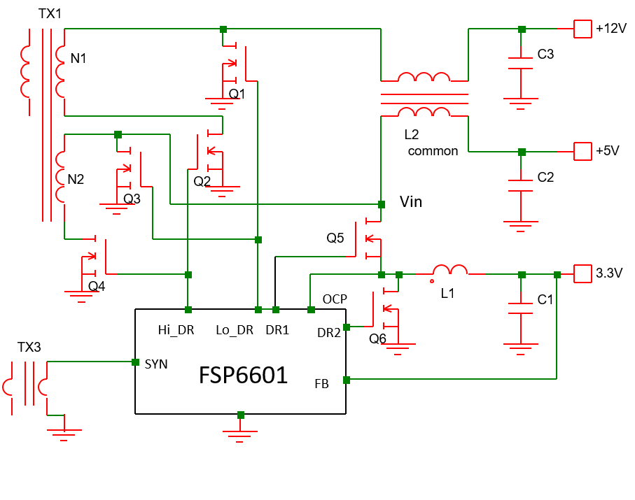
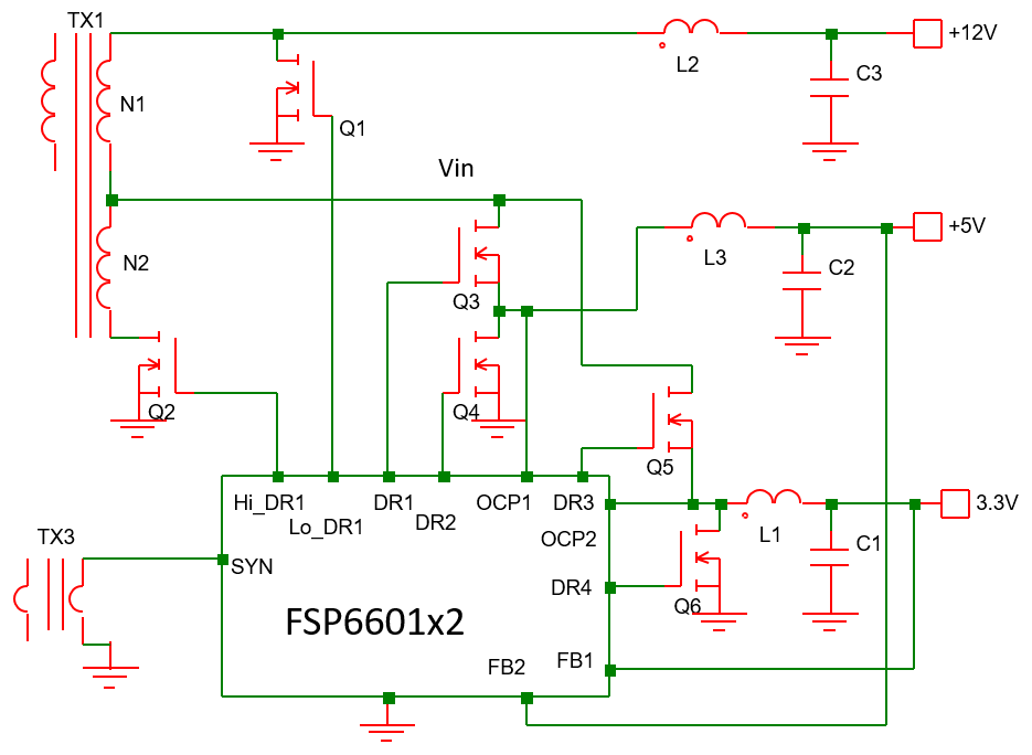
Figure 1 and Figure 2 show the pulse input DC to DC converter method used in Active-Clamp. The circuit design in Figure 1 is often used in specification requirements of output voltage precision of less than 5%. 12V and 5V feedbacks are tied together and share a common energy storage inductor, allowing 3.3V to adopt the pulse input DC to DC converter to achieve high-precision control. One FSP6601 control IC can be used. The circuit design framework in Figure 2 is used in high-end products with more stringent output voltage control precision requirements. The pulse source is tapped in the middle of the 12V transformer to provide 5V and 3.3V pulse input DC to DC conversion. Two FSP6601 control with IC design have independent feedback to achieve voltage high-precision requirements.
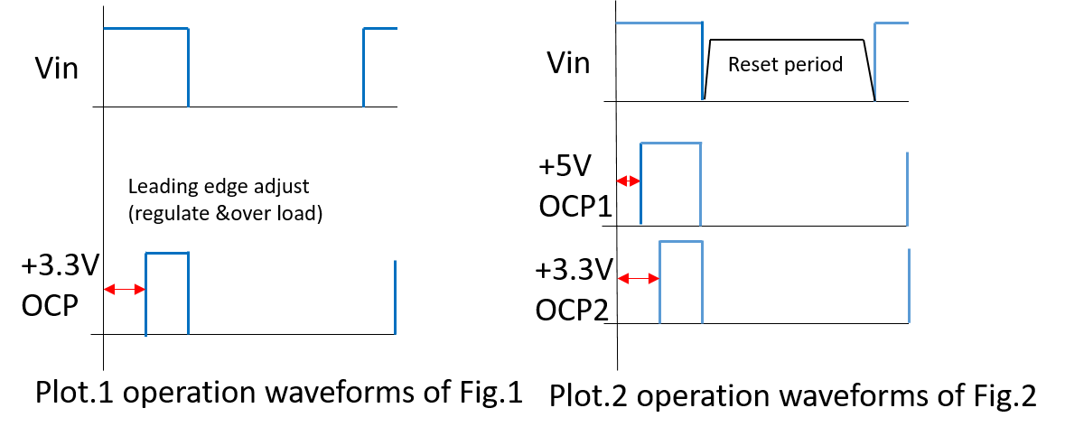
FSP Group has engaged in the research and development of dedicated IC for FSP6601 to meet the control technique requirement, in order to realize its applications. Since 5V and 3.3V currents do not pass the 12V inductor and capacitor, analysis shows that the advantages of adopting pulse input DC to DC converters are high efficiency without affecting 12V ripple performance. On top of it, the control technique involves the need to operate 12V output in a constant current mode, and the design must have reverse current limit function and be able to provide a stable pulse source under the circumstance of 12V without load (Vin). Furthermore, the 5V and 3.3V pulse modulation or overload control are by means of “leading edge”, because the control technique is not a function of a conventional DC to DC conversion controller. The above control technique proves that the adoption of pulse input DC to DC converters will not give rise to voltage stability problems in case of load bias.

Figure 1 : 12V&5V common,3.3V DC/DC

Figure 2 : 12V main, 5V&3.3V DC/DC
The operation waveforms in Figure 1 and Figure 2 can enhance understanding of the basic principle of pulse input DC/DC converters.

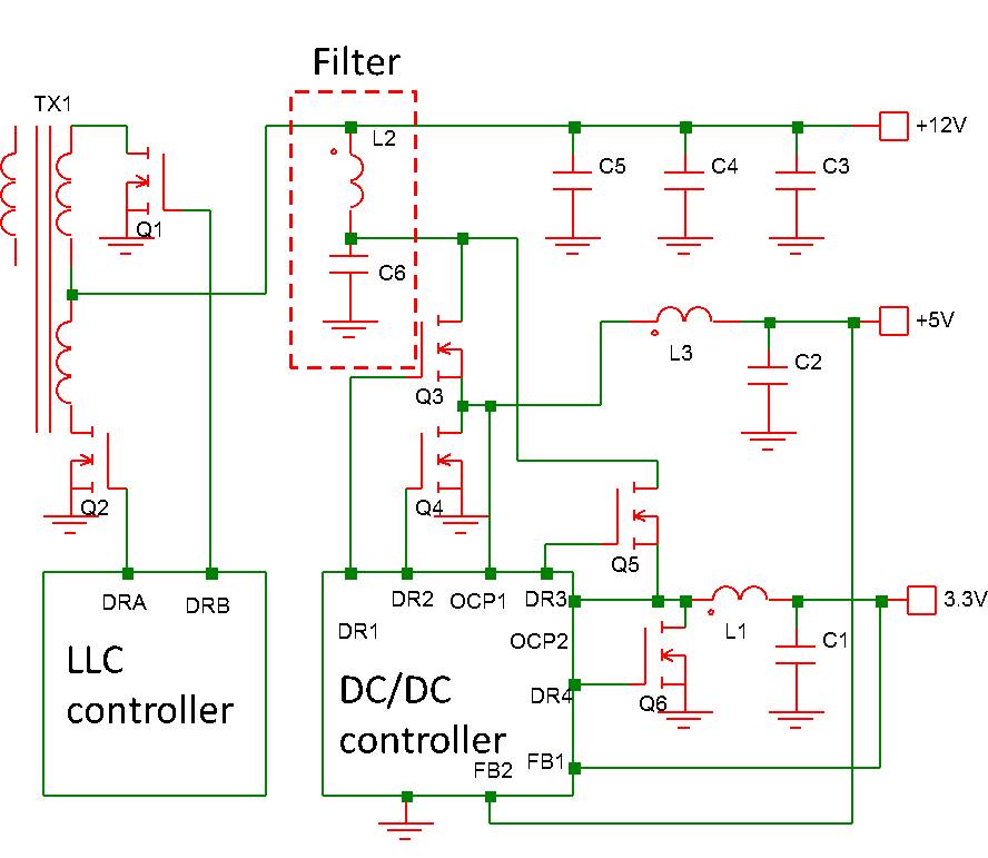
Another type is known as the DC input DC to DC converter. It can be used in the LLC circuit framework, converting 12V into 5V and 3.3V output (as shown in Figure 3). Basically, the 5V and 3.3V DC converter is added to 12V output, and 12V directly supplies current to the DC to DC converter. In consideration to the impact of the DC to DC converter pulse current on 12V ripple performance, a set of low-pass filter constituted by an inductor and a solid capacitor is usually added to improve the impacts caused by the ripples. However, low-pass filter will bring about additional loss and affect the overall efficiency.
In summary, it can be seen that the pulse input DC to DC converter used by the active clamp is not at all as simple as the magnetic amplifier design, neither are there phenomena of partial load or zero load. Its advantage is that it can improve efficiency without involving the complex DC input converter at the 12V end, thus technically making it a better circuit strategy.
Figure 3 : 12V to 5V &3.3V DC to DC converter under the LLC framework
FSP Group has a complete lineup of power supplies, and the Active-Clamp and LLC circuit designs have been widely applied within our product scope. The considerations of the output capacitor design are shared through objective commentaries.
관련 기사
FSP소개
세계 최고의 전원공급장치 제조업체인 FSP그룹은 1993년 설립 이래 '서비스, 전문, 혁신'이라는 경영 철학을 바탕으로 포괄적인 그린 에너지 솔루션 제품을 공급하고 있습니다.


